 Summary: This article compares isotropic and anisotropic silicon wafer etching processes, highlighting key differences, process parameters, practical benefits, and equipment considerations to help semiconductor professionals optimize manufacturing results.
Table of Contents
- Introduction
- Comparing Isotropic vs. Anisotropic Silicon Etching
- Wet Etching Process Parameters
- Advantages of Isotropic Silicon Etching
- Advantages of Anisotropic Silicon Etching
- Wet etching Equipment for Silicon Processing
- Choosing the Right Etching Method
- How Modutek Supports Isotropic and Anisotropic Etching Processes
- Conclusion
Introduction
Silicon wafer etching directly shapes the performance, precision, reliability, and overall efficiency of semiconductor devices and MEMS components. Selecting the optimal etching method and precisely managing critical parameters are essential to achieving high yields, cost-efficiency, and device integrity.
Process engineers and R&D professionals who thoroughly understand isotropic and anisotropic etching approaches and their respective advantages can better ensure consistent, high-quality results. This article compares isotropic and anisotropic silicon wafer etching processes, providing clear insights and practical guidance to help semiconductor professionals maximize process effectiveness and achieve targeted manufacturing outcomes.
Comparing Isotropic vs. Anisotropic Silicon Etching
Isotropic Etching Defined
Isotropic etching uniformly removes silicon material from exposed surfaces without dependence on crystal orientation. Even reaction rates lead to rounded profiles under mask edges.
Common isotropic etchants: HF, HNO₃, CH₃COOH (HNA mixture)
Key characteristics of isotropic etching include:
- Equal etch rates in all directions
- Rounded cavity profiles
- Significant undercut beneath masking layers
- Smooth surfaces, beneficial for specific optical applications
- Temperature-dependent reaction rates
Anisotropic Etching Defined
Anisotropic etching selectively removes silicon at varying rates based on crystal orientation, resulting in precise geometric structures. Silicon’s different bond densities across crystal planes allow for controlled directional etching.
Common anisotropic etchants: Potassium Hydroxide (KOH etching)
Key characteristics include:
- Direction-dependent etching rates influenced by crystal planes
- Minimal undercutting for high-resolution feature capability
- Predictable and repeatable profiles ideal for precision structures
- Typically has slower etch rates compared to isotropic removal
Critical Differences
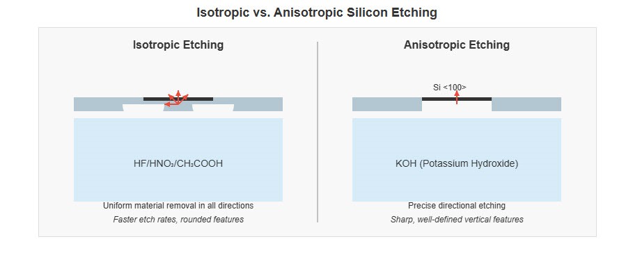
The fundamental distinction between these etching approaches lies in directional control. Isotropic etching removes silicon uniformly in all directions, which is ideal for rounded structures and bulk removal. Anisotropic etching selectively etches specific crystal orientations, facilitating precise, angular geometries.
Isotropic generally etches faster, suitable for rapidly creating larger, less critical geometries. Anisotropic etching presents controlled etching suited for intricate microstructures that demand accuracy. Understanding these differences helps you select the ideal etching process for your specific manufacturing application.
Summary of Key Differences
| Feature | Isotropic Etching | Anisotropic Etching |
| Geometry | Rounded, non-directional | Angular, direction-controlled |
| Etch Rate | Faster, suitable for bulk removal | Slower, precise detail formation |
| Undercutting | Significant | Minimal |
| Common Etchants | HNA mixtures (HF, HNO₃, CH₃COOH) | KOH |
Additional details on isotropic and anisotropic etching can be found in the following documentation:
- Silicon Wet Isotropic and Anisotropic Etching, University of Maryland
- Anisotropic Silicon Etch Using KOH, University of California at Irvine
Wet Etching Process Parameters
Optimizing etching process parameters directly affects device quality, manufacturing speed, and accuracy. Precise control over etching parameters ensures repeatable results.
Important Parameters for Reliable Etching Results:
- Temperature Control: Even small (~10°C) temperature changes can double etch rates. Consistent temperature ensures reliable performance and stable results.
- Chemical Concentration: Accurate chemical mixtures are crucial (ensures repeatability in process quality).
- Agitation: Uniform solution movement maintains consistent chemical interaction (ensures predictable etching outcomes on each wafer)
- Chemical Additives: Specialized additives stabilize reactions (improving selectivity, surface smoothness, and device reliability)
Process Parameter Differences: Isotropic vs. Anisotropic
| Parameter | Isotropic Control Strategy | Anisotropic Control Strategy |
| Temperature | Moderate temperature, tight control (±0.5°C) | Elevated temperatures (70-85°C), stable through process cycle |
| Chemical Concentration | Precise HNA mixture ratios | Consistent KOH concentrations (30-40%) |
| Agitation | Moderate, uniform agitation for even etchant contact | Defined fluid dynamics for consistent directional control |
| Timing | Determined by desired total feature depth | Guided by crystal plane etch rates |
The wafer fabrication equipment used in etching processes must precisely control these parameters to ensure consistent, repeatable etching results across production runs.
Advantages of Isotropic Silicon Etching
Isotropic etching achieves unique geometric profiles and efficiencies beneficial to specific semiconductor applications. These include the following:
Uniform Material Removal Benefits Include:
- Rounded Profiles: Improve MEMS reliability and extend device lifespan by reducing mechanical stress.
- Higher Throughput Rates: Accelerate production cycles through rapid silicon bulk removal.
- Optimized Fluid Dynamics: Enhance MEMS and microfluidic device performance through smoother, more efficient fluid channels.
- High Selectivity: Protect critical device structures by removing materials precisely without collateral damage.
Common Applications in Semiconductor Fabrication
Isotropic silicon etching finds widespread use across multiple applications that include:
MEMS Device Applications
- Pressure sensors with flexible membranes
- Accelerometers with mass-spring structures
- Microfluidic channels with controlled fluid dynamics
- Optical MEMS with curved reflective surfaces
Semiconductor Device Applications
- Flash memory cell formation
- Trench capacitor structures
- Silicon-on-insulator (SOI) layer thinning
- Wafer backside preparation
Research and Development Applications
- Rapid prototyping of device structures
- Material characterization studies
- Process development experiments
- Novel device architecture exploration
For research laboratories and process development teams, isotropic etching provides particular value through its simplicity, rapid material removal capabilities, and ability to create structures that are difficult to achieve with other techniques. Isotropic applications require specialized equipment for precise temperature control and chemical management to ensure consistent results. Wafer fabrication equipment must be properly configured to maintain stable process conditions throughout the etching cycle.
Advantages of Anisotropic Silicon Etching
Anisotropic silicon etching delivers exceptional precision for applications requiring well-defined geometric structures with straight sidewalls and angular features.
Anisotropic Etching delivers clear strategic benefits:
- Precisely Defined Features: Ensures exact dimensions essential for precise semiconductor circuits.
- Minimal Undercutting: Supports denser component layouts and increased design flexibility, improving device miniaturization.
- Predictable, Consistent Profiles: Reduces process variability, ensuring high repeatability and enhancing overall product yield and quality.
These characteristics make anisotropic etching invaluable for high-precision applications where feature dimensions directly impact device performance.
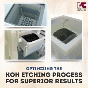
The Role of KOH Etching in Anisotropic Structures
KOH etching is the industry standard for anisotropic silicon etching due to its well-characterized performance. KOH solutions provide remarkable etch rate differentials between crystal planes, with <100>:<111> selectivity of approximately 400:1 at elevated temperatures.
This extreme selectivity enables the creation of structures impossible with other methods, including ultra-thin membranes bounded by <111> planes that act as natural etch stops. The KOH wafer etching process offers numerous practical benefits, including self-limiting geometries, highly repeatable results, and precise depth control.
Specific applications enabled by KOH anisotropic etching include radiation-hardened circuits, JFET arrays, solar cell anti-reflecting surfaces, waveguides, infrared detectors, high-value capacitors, and black bodies.
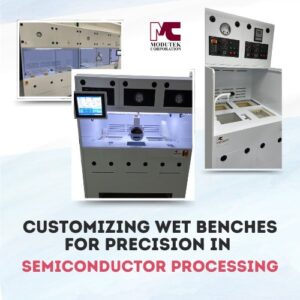
Wet Etching Equipment for Silicon Processing
Achieving consistent, high-quality results in silicon etching relies heavily on selecting the right equipment integrated within wet bench systems. Specialized and reliable wet processing equipment enables precise control over chemical mixtures, accurate temperature management, and careful wafer handling, essential to both isotropic and anisotropic silicon wafer etching processes. Modutek offers comprehensive wet processing equipment designed specifically for silicon wet etching applications in both manufacturing facilities and R&D laboratories.
Essential Equipment within Wet Bench Systems
Effective wet bench stations typically include specialized components for both isotropic and anisotropic etching, including:
- Chemical Baths and Tanks: Corrosion-resistant baths and process tanks made of quartz, Teflon®, or polypropylene contain aggressive chemicals safely. Quartz or polypropylene tanks are typically preferred for isotropic acids (e.g., HNA mixtures), while Teflon® or polypropylene tanks are optimal for anisotropic KOH etching processes.
- Precision Temperature Controllers: Temperature control circulators ensure tight temperature variances within ±0.5°C, critical for stable results. Accurate temperature control is especially crucial for anisotropic KOH etching, which requires higher, consistent temperatures (70-85°C), and for isotropic etching methods requiring moderate, well-controlled temperature ranges.
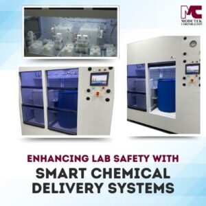
- Chemical Delivery and Concentration Monitoring: Automated chemical systems precisely manage etchant concentrations, replenishing solutions automatically to prevent process drift. This capability is critical for both isotropic etching (accurate HNA ratio mixtures) and anisotropic etching processes (maintaining 30-40% KOH concentrations).
- Wafer Handling and Carrier Systems: Safe, contamination-free wafer transfer and positioning systems significantly improve efficiency, repeatability, and yield. Manual, semi-automated, or fully robotic wafer handling is integrated based on process complexity and volume requirements.
- Process Automation and Control Systems: Programmable logic controllers (PLC), automated timing systems, and integrated recipe management guarantee that etching parameters remain consistent, reproducible, and easily adjustable for both isotropic and anisotropic processes.
- Quick Dump Rinsers (QDR) and Dryers: Integrated rinsers and drying equipment (spin dryers or IPA dryers) effectively remove residual chemicals after etching, preserving wafer integrity and cleanliness critical to semiconductor device fabrication.
- Safety and Containment Solutions: Chemical-resistant enclosures, spill containment trays, exhaust fume hoods, leak detectors, emergency shutoff interlocks, and ergonomically designed process stations ensure user safety, chemical containment, and regulatory compliance.
Specific Modutek Wet Processing Equipment for Wet Etching Methods
Modutek provides comprehensive wet bench solutions explicitly tailored to isotropic and anisotropic wafer etching processes:
Equipment Supporting Anisotropic Silicon Etching:
 Temperature-controlled Teflon® Tanks: Designed specifically for high-temperature KOH etching, these robust tanks resist aggressive caustic solutions, ensuring long-term reliability and safety.
 Temperature-controlled Teflon® Tanks: Designed specifically for high-temperature
 - Fully Automated or Semi-Automated Wet Benches:Ideal for precision anisotropic wafer etching, these systems offer accurate temperature control, chemical delivery, precise timing, dependable repeatability, and minimized human intervention. These systems incorporate robotic wafer handling, integrated metrology, closed-loop parameter control, recipe management systems, and statistical process control integration.
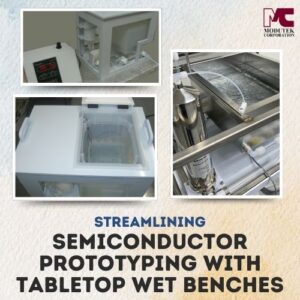
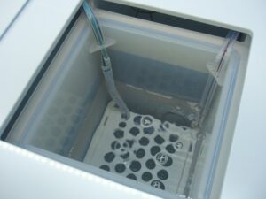
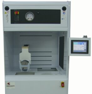
- Wet Processing Tabletop Bath Systems: Modutek’s tabletop wet processing baths offer R&D professionals compact, flexible platforms ideal for precise anisotropic KOH etching experiments with stable, reliable parameter control.
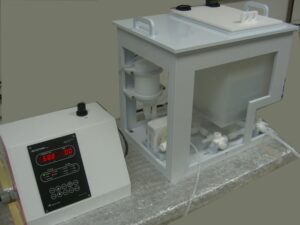 Wet Processing Tabletop Bath Systems:
 Equipment Supporting Isotropic Silicon Etching:
- Quartz and Polypropylene Chemical Baths: Modutek’s Quartz Tanks are compatible with isotropic etching chemistries (e.g., HF, HNO₃, CH₃COOH mixtures), these chemically resistant process tanks provide durability and accurate chemical containment.
 Manual and Semi-Automated Wet Bench Stations: Provide flexibility and lower-cost operation suitable for isotropic etching tasks involving bulk silicon removal or rapid wafer thinning operations.
- Chemical Delivery and Mixing Systems: Equipped for precise mixing and composition replenishment of common isotropic etchants, handling accurate chemical ratios consistently to maintain predictable uniform results.
 Manual and Semi-Automated Wet Bench Stations: Provide flexibility and lower-cost operation suitable for isotropic etching tasks involving bulk silicon removal or rapid wafer thinning operations.
Key Considerations When Selecting Wet Etching Equipment
Choosing wet bench systems and associated wet etching equipment involves evaluating critical factors such as:
- Chemical Compatibility: Resistant materials are critical to safely manage aggressive isotropic or anisotropic etchants without contamination.
- Precise Temperature Control: Accurate temperature stability significantly impacts etching results, particularly vital for the controlled reactions of KOH and other anisotropic etchants.
- Automation and Control Capabilities: The automation level (manual, semi-automated, or automated) must align with production volume, process complexity, and precision requirements.
- Cleanliness and Contamination Control: Semiconductor environments require rigorous sanitation standards to prevent contamination and enhance yield quality.
- Reliability and Longevity: Durable construction and redundant system protections extend equipment life and reliability, reducing downtime and total operational cost.
By utilizing precision-engineered wet processing equipment carefully designed and configured for either isotropic or anisotropic wafer etching processes, semiconductor manufacturers and R&D laboratories can reliably achieve high-quality device structures, precise etched profiles, and consistent manufacturing outcomes. Modutek’s extensive experience and customized solutions support both research-focused experimentation and high-volume production applications, ensuring processes run reliably with optimal efficiency, safety, and repeatability.
Choosing the Right Etching Method
Choosing the correct etching method directly impacts product performance and manufacturing cost-effectiveness. Selecting isotropic or anisotropic etching should be driven by specific device requirements and other critical factors.
Material Properties and Structure Requirements
The optimal etching method depends heavily on the device’s final desired properties. Consider these common feature requirements when selecting the best etching method:
| Feature Requirement | Preferred Etching Approach |
| Vertical sidewalls | Anisotropic (KOH on <110> silicon) |
| Rounded cavities | Isotropic (controlled HNA mixtures) |
| High aspect ratios | Anisotropic (optimized crystal orientation/depth) |
| Curved profiles | Isotropic (balanced undercut control) |
| Thin membranes | Anisotropic (leverage crystal-plane etch stops) |
| Bulk removal tasks | Isotropic (faster, uniform silicon removal) |
Resolution and Cost Factors
- Fine Resolution: Typically favors anisotropic processes due to controlled undercut and precision.
- Cost Sensitivity: Isotropic often has lower chemical and operational complexity, suitable for non-critical structures and prototyping.
- Process Complexity: Anisotropic processes demand detailed crystal orientation knowledge, which impacts training and equipment needs.
Application-Specific Guidance
Research and Development Settings
R&D environments benefit from flexibility, equipment versatility, parameter exploration capabilities, and efficient small-batch handling. In research settings, systems supporting both etching methodologies provide maximum flexibility.
Manufacturing Environments
Production facilities prioritize process stability, throughput maximization, yield consistency, and cost efficiency. Manufacturing operations typically benefit from purpose-optimized systems focused on specific etching approaches matched to production requirements.
How Modutek Supports Isotropic and Anisotropic Etching Processes
With over 40 years of experience in wet process equipment manufacturing, Modutek offers specialized solutions for semiconductor manufacturing and R&D facilities requiring precise silicon etching capabilities.
Customizable Wet Etching Systems
Modutek’s engineering expertise in wet processing equipment is tailored to support specific etching requirements:
Research-Optimized Systems
For R&D environments, Modutek offers manual wet benches supporting multiple process chemistries, and laboratory-scale wet processing tabletop bath units for space-constrained facilities, flexible configuration options, and modular expansion capabilities.
Production-Ready Solutions
For manufacturing operations, Modutek delivers high-throughput automated wet bench systems and semi-automated wet bench systems with integrated wet processing equipment and chemical delivery systems.
Precise Process Control Capabilities
Achieving repeatable etching results requires exacting control over critical parameters:
Temperature Management Systems
Modutek’s wet processing temperature control circulators provide ±0.5°C stability for critical etching processes, PID-controlled heating with rapid response, uniform bath temperatures, and over-temperature protection.
Chemical Management Integration
Comprehensive chemical handling features include automated delivery systems, concentration monitoring capabilities, filtration systems, and chemical recirculation options.
Process Automation Options
Scalable automation capabilities span from basic programmable controllers to comprehensive data logging, recipe management, and integration systems.
Commitment to Reliability, Safety, and Support
Modutek’s systems incorporate multiple features ensuring long-term performance including corrosion-resistant materials, industrial-grade components, redundant critical systems, and field-serviceable designs. Safety features encompass fume containment, emergency shutdown capabilities, leak detection, and comprehensive interlocks.
For both research laboratories and production facilities, Modutek’s wet processing equipment delivers the precision, reliability, and flexibility required for advanced semiconductor applications.
Conclusion
Choosing between isotropic and anisotropic silicon wafer etching methods directly shapes device functionalities, manufacturing efficiency, and cost-effectiveness.
- Isotropic methods optimize efficiency for bulk silicon removal, rounded features, and non-critical tasks.
- Anisotropic methods deliver precise designs, critical geometries, minimal undercutting, and repeatability.
Determining the ideal wafer etching process requires a detailed assessment of production goals, device requirements, manufacturing volume, and complexity management strategies. Modutek supports semiconductor manufacturers and researchers by providing specialized wet etching equipment designed explicitly around unique processing needs, delivering precision, consistency, and quality.
Next Steps:
Contact Modutek for a free consultation to discuss your process requirements. Modutek’s in-house engineering team will work directly with you to design customized wet processing equipment to improve yield, reduce costs, and achieve manufacturing goals.