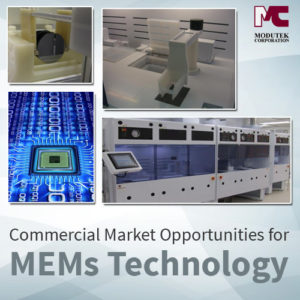
 Micro-electro-mechanical systems (MEMS) is a technology that incorporates the use of microscopic devices ranging in size from several millimeters to less than one micron. They usually have both electrical and mechanical functions and often include parts that can move in response to process conditions, commands from outside the structure or commands from integrated electronics. Typical miniaturized MEMS devices include sensors, actuators and other microscopic structures manufactured on silicon wafers using similar techniques as for semiconductors. They are popular because they are inexpensive to fabricate and are easily integrated into systems containing electronic controls, often on the same silicon wafer.
MEMS Applications
MEMS were first used in the automotive industry and then found increased application in the medical and optical fields. Typical macroscopic functions that were taken over by MEMS counterparts were pressure sensors, inertial sensors and chemical sensors. The MEMS sensors were less expensive to manufacture and performed better than the corresponding large sensors. In addition, different sensors could be placed on one silicon wafer along with signal processing electronics. For example, one unit could measure chemical pressure, detect impurities and generate alarm signals.
As MEMS fabrication methods became more sophisticated, the systems were able to take on additional functions and include different structures. For example, today’s MEMS can include mirrors, gears, pumps, nozzles and valves. Associated electronics can evaluate the signals, perform complex analysis and send results to external receivers via radio frequency elements. Such devices are found in the automotive industry in car airbags, tires and fuel systems. Technical products such as ink jet printers, digital projectors, bar code readers and display screens use MEMS to reduce costs and miniaturize components. Medical systems and devices use the miniature MEMS for diabetic evaluation, insulin delivery, blood analysis and needle less injectors. As the number of applications increases, the market for MEMS continues to grow as does the interest in inexpensive, reliable and rapid fabrication methods.
How MEMS are Produced
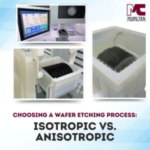
To create the microscopic structures that make up MEMS, manufacturers use technology similar to that used to produce microelectronics. For silicon wafer based MEMS, the wafers are masked, etched and cleaned in multiple steps. Silicon wet etching is one method that offers a number of advantages.
Wet etching with potassium hydroxide, or KOH etching, is inexpensive and reliable. KOH is safe and etches quickly. Repeatability is good and the process can be controlled by changing the temperature, the concentration of KOH, the crystal plane orientation of the silicon and the doping concentration. The KOH process allows for very precise etching and it can be automated. Other methods of creating microscopic structures on silicon wafers are more expensive, more risky or not as reliable.
Modutek’s Support for the KOH Etching Process
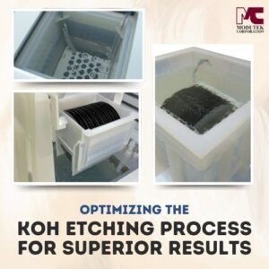
Modutek offers a variety of wet bench processing options including KOH etching. The company’s KOH silicon etching tank is designed and manufactured in house and can be built to customer specifications to satisfy specific wet process requirements. Its design emphasizes cleanliness with an all-PFA construction and consistency in the process to deliver accurate etching results.
The tanks are manufactured to reduce impurities and contaminants to a minimum with the PFA sheet material welded together using advanced welding techniques. The resulting process tanks deliver excellent performance and high quality output. Custom installations to work with existing wet bench equipment are available. Modutek uses its experience in the wet bench process to ensure that customer needs are met and the equipment functions as expected. If you have challenging wet processing applications contact Modutek for a free quote or consultation on solutions that will address your requirements.


