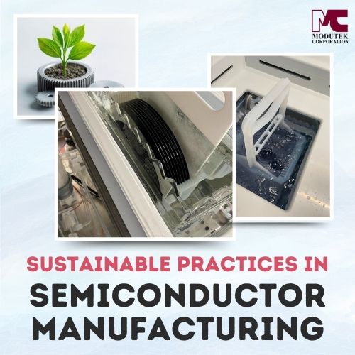
 Using sustainable practices with innovative technologies has become a critical priority in semiconductor manufacturing. The industry’s environmental footprint, driven by extensive resource use and waste generation, necessitates the adoption of eco-friendly practices. Semiconductor manufacturers and research facilities increasingly integrate sustainable methodologies such as waste reduction, energy efficiency, and the elimination of solvents to mitigate environmental impact. Central to these efforts are innovative cleaning processes, including the ozone cleaning process and megasonic cleaning, which play critical roles in eliminating solvents, reducing chemical usage, and conserving water. These sustainable practices align with environmental regulations and enhance operational efficiency and cost-effectiveness, making them indispensable for modern semiconductor facilities.
Understanding Sustainable Practices in Semiconductor Manufacturing
Sustainable practices in semiconductor manufacturing are essential for minimizing the environmental impact of this resource-intensive industry. Implementing these practices addresses various challenges, including significant energy consumption, hazardous waste generation, and substantial water use.
Significance of Sustainable Practices
The semiconductor industry is characterized by complex processes that require large amounts of energy and chemicals, leading to a considerable environmental footprint. Sustainable practices help mitigate these impacts by promoting efficient resource use and reducing waste. These practices contribute to environmental preservation and align with regulatory compliance, ensuring that manufacturing facilities meet stringent environmental standards. By integrating sustainable methods, semiconductor manufacturers can enhance their corporate social responsibility profiles, attract environmentally conscious customers, and gain a competitive edge.
Current Challenges
The semiconductor manufacturing sector faces several challenges in implementing sustainable practices. These include:
- Energy Consumption: The manufacturing process involves high energy usage, particularly in the production and cleaning stages. Reducing energy consumption without compromising efficiency is a significant challenge.
- Chemical Use and Waste: The industry relies heavily on various chemicals and solvents, leading to hazardous waste generation. It is crucial to reduce and dispose of this waste in an environmentally friendly manner.
- Water Usage: Semiconductor manufacturing is water-intensive, and wafer cleaning processes and chemical dilution require large volumes of water. Reducing water usage and promoting water recycling are key areas of focus.
Addressing the Challenges
To address these challenges, the industry has developed several sustainable practices:
- Energy Efficiency: Implementing energy-efficient technologies and processes, such as megasonic cleaning, which uses high-frequency sound waves to clean wafers, significantly reduces energy consumption compared to traditional methods.
- Waste Reduction: Techniques such as bleed and feed for chemical baths minimize the use of chemicals and reduce waste. For example, in the Piranha etch process, this technique ensures effective cleaning with lower chemical consumption.
- Eliminate Solvents and Reduce Water Usage: The ozone cleaning process eliminates the need for using solvents and reduces water usage.
By implementing these sustainable practices, semiconductor manufacturers can significantly reduce their environmental impact while maintaining high production standards and efficiency. These practices benefit the environment and offer economic advantages through cost savings and improved regulatory compliance.
Waste Reduction Techniques
Waste reduction is crucial in sustainable semiconductor manufacturing. By minimizing waste, manufacturers can lower their environmental impact and enhance operational efficiency. Key waste reduction techniques include filtering with recirculation pumps in wet processing baths and the bleed and feed method for reducing chemical usage, particularly in the Piranha etch process.
Filtering Using Recirculation Pumps in Wet Processing Baths
Recirculation pumps in wet processing baths continuously filter and recirculate chemical solutions used in cleaning and etching processes. This method maintains the quality and effectiveness of the chemicals over longer periods, reducing the need for frequent disposal and replenishment.
Benefits:
- Extended Chemical Life: Maintains chemical efficacy, extending the lifespan of solutions.
- Reduced Waste: Minimizes hazardous waste generation.
- Cost Savings: Lowers operational costs through reduced chemical consumption.
Bleed and Feed Using Less Chemicals
The bleed and feed technique periodically removes a small portion of the used chemical solution (bleed) and replaces it with fresh chemicals (feed). This maintains the necessary chemical concentration and quality without complete solution replacement.
Application in the Piranha Etch Process
The Piranha etch process, which cleans silicon wafers, benefits from the bleed and feed technique. This process typically uses a mixture of sulfuric acid and hydrogen peroxide to remove organic residues. By applying bleed and feed, manufacturers maintain the effectiveness of the etch solution over an extended period, reducing chemical usage and waste.
Benefits:
- Cost Savings: Reduces operational costs by lowering chemical consumption.
- Reduced Chemical Usage: Minimizes the need for frequent chemical replenishment.
- Enhanced Efficiency: Ensures consistent and effective cleaning performance by maintaining optimal chemical concentration.
The Bleed and Feed Technique Used for Piranha Etch
Modutek’s implementation of the bleed and feed technique for the Piranha etch process has shown significant reductions in chemical usage and waste, contributing to more sustainable manufacturing operations.
Semiconductor manufacturers and research centers can achieve significant environmental and economic benefits by adopting these waste reduction techniques. Filtering with recirculation pumps and the bleed and feed method minimizes waste, lowers costs, and enhances manufacturing sustainability.
Energy Efficiency and Reducing Chemicals in Cleaning
Enhancing energy efficiency and reducing chemical usage in wafer processing is pivotal in promoting sustainability within semiconductor manufacturing. Modern cleaning techniques, such as megasonic cleaning, significantly contribute to these objectives by minimizing the environmental footprint and operational costs.
Megasonic Cleaning
Megasonic cleaning employs high-frequency sound waves to clean semiconductor wafers, providing an advanced and eco-friendly alternative to traditional cleaning methods. This process involves the generation of sound waves in the megasonic range (typically at and above 1 MHz), which create microscopic bubbles in the cleaning solution. When these bubbles collapse, they produce localized high-energy jets that effectively remove contaminants from the wafer surfaces. Modutek uses megaonic cleaning systems from Kaijo Shibuya, a leading provider of advanced meagasonic and ultrasonic cleaning technology.
Benefits:
- Reduced Chemical Usage: Unlike conventional methods that rely heavily on chemicals, megasonic cleaning significantly lowers the need for chemical agents. This reduction decreases the volume of hazardous waste and lessens the environmental impact.
- Energy Efficiency: Megasonic cleaning is inherently more energy-efficient. The high-frequency sound waves require less energy to maintain effective cleaning action compared to the thermal and mechanical energy demands of traditional methods.
- Superior Cleaning Performance: The precision and effectiveness of megasonic cleaning ensure thorough removal of submicron particles and organic contaminants, enhancing the quality of semiconductor products.
- Extended Equipment Lifespan: By reducing the need for harsh chemicals, megasonic cleaning minimizes the wear and tear on cleaning equipment, extending its operational lifespan.
Incorporating Megasonic Cleaning in Modutek’s Wet Benches
Incorporating megasonic cleaning in wet bench systems has substantially improved environmental and operational performance for Modutek’s customers. By implementing this technology, Modutek’s systems have achieved notable reductions in chemical usage and energy consumption, aligning with its sustainability goals.
Advantages Over Traditional Cleaning Methods:
- Environmental Impact: With fewer chemicals and lower energy requirements, megasonic cleaning significantly reduces the environmental footprint of the cleaning process.
- Cost Savings: The efficiency of megasonic cleaning translates into lower operational costs, offering economic benefits alongside environmental advantages.
By integrating megasonic cleaning into semiconductor manufacturing processes, companies can achieve enhanced energy efficiency and reduced chemical usage. This advanced cleaning technology supports environmental sustainability and ensures high product quality and operational efficiency standards.
Eliminating Solvents and Reducing Water and Chemicals Usage
Eliminating solvents and reducing water and chemical usage are critical for achieving sustainable operations in the semiconductor manufacturing industry. Innovative cleaning processes, such as the ozone cleaning process, play a significant role in minimizing resource consumption and environmental impact.
Ozone Cleaning Process
The ozone cleaning process is a highly effective and environmentally friendly method for cleaning semiconductor wafers. This technique uses ozone gas dissolved in water to create a powerful oxidizing solution that breaks down organic contaminants into carbon dioxide and water. The process is highly efficient and significantly eliminates the need for traditional chemical solvents.
Benefits:
- Elimination of Solvents: Ozone cleaning replaces the need for traditional solvents, reducing the volume of hazardous chemicals used in the cleaning process.
- Reduced Chemical Usage: The process utilizes ozone, decreasing the overall reliance on chemical agents and thereby reducing hazardous waste generation.
- Water Conservation: The process uses less water compared to traditional cleaning methods, contributing to significant water savings.
- Enhanced Cleaning Efficiency: Ozone’s strong oxidizing properties ensure thorough removal of organic contaminants, resulting in cleaner wafer surfaces.
- Safety and Environmental Impact: Ozone decomposes into oxygen, leaving no harmful residues, making it a safer and more environmentally friendly option.
Role in Eliminating Solvents
The ozone cleaning process is particularly beneficial in eliminating the use of solvents. Ozone’s ability to oxidize and break down contaminants means that traditional solvents are no longer required, resulting in a safer and more sustainable cleaning method. This reduces chemical usage and minimizes the environmental and health risks associated with solvent handling and disposal.
Using the Ozone Cleaning Process in Modutek’s Wet Benches
Modutek’s implementation of the ozone cleaning process has significantly improved environmental sustainability and operational efficiency for its customers. By integrating ozone cleaning into its wet bench systems, Modutek has helped clients eliminate the use of solvents and achieve substantial reductions in chemical and water usage, promoting a more sustainable manufacturing environment.
By adopting the ozone cleaning process, semiconductor manufacturers can significantly reduce their environmental impact while enhancing efficiency. These practices align with the industry’s commitment to sustainability and demonstrate a proactive approach to resource management. Modutek’s dedication to these innovative solutions exemplifies the benefits of integrating eco-friendly technologies in semiconductor manufacturing, paving the way for a greener and more efficient future.
Integrating Sustainable Practices into Facility Operations
Implementing sustainable practices in semiconductor manufacturing facilities requires a strategic approach that includes process optimization, employee training, and advanced technologies. This integration enhances environmental performance, ensures regulatory compliance, and improves operational efficiency.
Practical Steps for Implementation
- Assessment and Planning: Assess current operations to identify improvement areas and develop a sustainability plan with specific goals and metrics.
- Technology Integration: Incorporate advanced technologies like megasonic and ozone cleaning processes to reduce chemical and water usage while improving efficiency.
- Waste Reduction Techniques: Use methods such as filtering with recirculation pumps and the bleed and feed method to minimize waste and extend the lifespan of chemicals.
- Energy Efficiency Measures: Invest in energy-efficient equipment and optimize processes to reduce energy consumption, complemented by regular maintenance.
- Water Conservation: Adopt water-saving practices, such as reusing cleaning solutions, to reduce the facility’s water footprint.
- Employee Training and Engagement: Provide comprehensive training programs to ensure employees understand and implement sustainable practices, fostering a culture of sustainability.
Modutek’s Support for Sustainable Practices
Modutek supports semiconductor manufacturers with products and services designed to enhance sustainability:
- Customized Solutions: Tailored solutions meet specific facility needs, ensuring optimal integration of sustainable practices.
- Expert Consultation: Consultation services help facilities identify improvement opportunities and develop effective sustainability strategies.
- Training Programs: Comprehensive training ensures facility personnel are well-equipped to implement and maintain sustainable practices.
By following these steps and leveraging Modutek’s expertise, semiconductor manufacturers and research facilities can successfully integrate sustainable practices, enhancing environmental performance and operational efficiency for a more sustainable future.
The Bottom Line
Implementing sustainable practices in semiconductor manufacturing is essential for reducing environmental impact and enhancing operational efficiency. Techniques such as megasonic and the ozone cleaning process, waste reduction methods, and energy and water conservation play crucial roles. Modutek supports these initiatives with tailored equipment solutions that support your unique wafer processing requirements. The advanced technologies and waste reduction techniques that Modutek provides have helped customers significantly reduce chemical and water usage, lower operational costs, and improve regulatory compliance. Contact Modutek for a free consultation to discuss systems and equipment that can be used to support sustainable practices at your facility.